

News
Featured

Contact Us
Contact: POWER DUKE
Phone: +86 18059884790
E-mail: plc66@qq.com
Add: fujian xiamen
- Warehouse: Spot
- Warranty: 365 days
- Quality: Original module
- Condition: New
- Shipping method: Courier delivery
- Contact person: LI MING
- Contact number: +86 18059884790
- WeChat:18059884790
- E-mail: plc66@qq.com
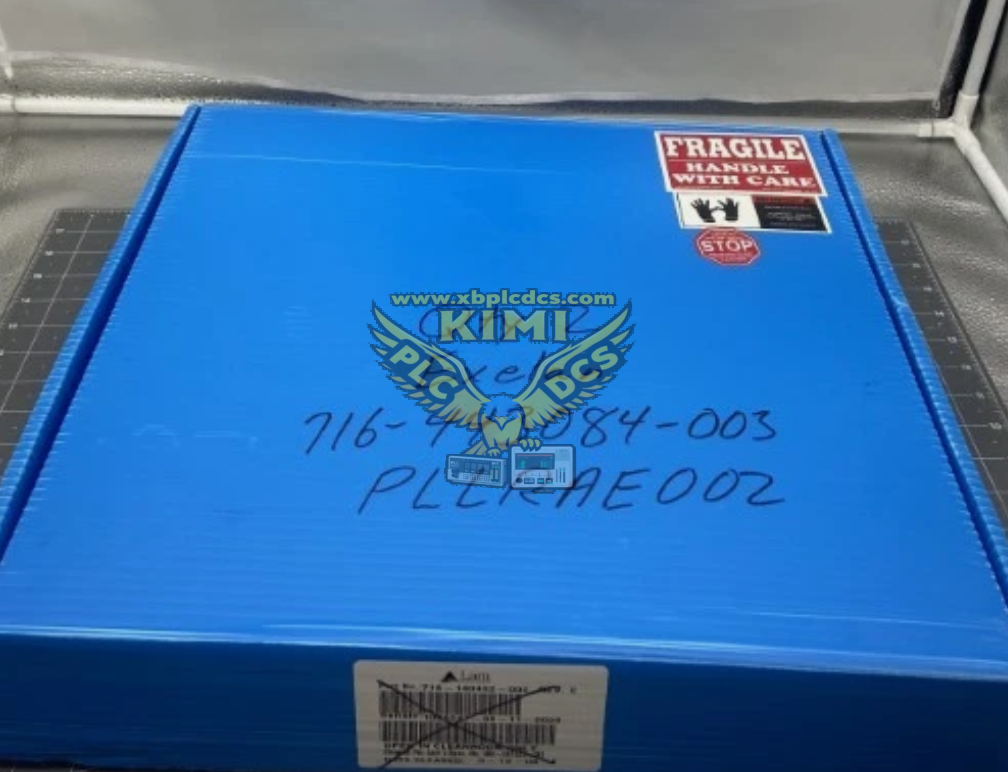
LAM 716-443084-003 Bottom Confinement Ring
1. Product Description
716-443084-003 is OEM ceramic Bottom Confinement Ring exclusively developed by Lam Research for 150mm (6-inch) ICP plasma etching chambers, matched as a pair with Top Confinement Ring 716-443083-004 and Upper Gas Inlet Ring 716-443090-002 to form a complete plasma confinement assembly inside vacuum process cavities. It is mounted on the edge of electrostatic chuck (ESC), forming the bottom boundary of the plasma reaction zone directly surrounding the wafer perimeter.
- High-density high-purity ceramic substrate with dense anti-sputtering protective coating, resistant to continuous bombardment of fluorine/chlorine corrosive plasma chemistries.
- Precision machined annular profile with controlled vertical gap clearance cooperating with top confinement ring to define closed plasma reaction space above 150mm silicon wafers.
- Built-in positioning notches and flat sealing lands for accurate alignment and vacuum sealing with ESC and top confinement components during chamber assembly.
- Stable thermal expansion coefficient to maintain fixed confinement gap geometry under repeated high-low temperature cycling during mass production batches.
- Strict cleanroom-level dimensional tolerances to eliminate asymmetric gas pumping and radial plasma density deviation across wafer surface.
Designed for legacy Lam 150mm etch platforms, applicable to dielectric, polysilicon gate and shallow trench isolation (STI) etching processes.
2. Core Product Functions
- Closed Plasma Boundary Forming: Matches with top confinement ring to construct an enclosed plasma reaction cavity, restricts high-density plasma above wafer surface and suppresses lateral plasma leakage to chamber side liners, reducing parasitic sidewall etching defects.
- Wafer Edge Plasma Tuning: Precisely adjusts plasma density at wafer edge perimeter to balance center-edge etch depth uniformity, eliminate edge rounding, trench offset and micro-loading effects.
- Uniform Exhaust Gas Flow Control: Cooperates with top ring radial gap channels to balance vacuum pumping velocity across wafer radius, stabilize chamber pressure and avoid pressure gradient induced process drift.
- RF Electric Field Homogenization: Acts as dielectric barrier to smooth RF electric field distribution, suppress localized high plasma density and reduce intermittent plasma arc discharge during recipe switching.
- Particle Contamination Reduction: Wear-resistant coating minimizes ceramic substrate sputtering and polymer byproduct accumulation, lowering wafer particle defect rate during long-term production campaigns.
- Process Repeatability Stabilization: Fixed gap geometry maintains consistent gas flow impedance batch-to-batch, ensuring stable etch profile without frequent gas flow and RF matching re-calibration.
3. Typical Application Scenarios
- Lam Research 150mm inductively coupled plasma (ICP) etch chambers for legacy logic, memory and power semiconductor wafer manufacturing.
- High-aspect ratio dielectric etching, polysilicon gate etching and shallow trench isolation process chambers requiring strict plasma uniformity control.
- Semiconductor cleanroom mass production fabs with continuous 150mm wafer batch processing under high RF power plasma operating environments.
- Chamber preventive maintenance (PM) spare replacement to restore plasma confinement performance after long-term plasma erosion and coating degradation.
- Full set gas-plasma confinement assembly matching with 716-443083-004 top confinement ring and 716-443090-002 upper gas inlet ring.
4. Common Issues & Troubleshooting
Issue 1: Severe center-edge etch rate non-uniformity on 150mm wafers
Root Causes: Polymer residues clogging peripheral confinement gaps, uneven plasma sputtering widening bottom ring clearance, misaligned installation offsetting gap symmetry. Solutions: Perform wet chemical stripping to clean all flow channels, inspect coating erosion depth, re-lock alignment notches fully onto ESC mounting surface.
Issue 2: Sharp rise in wafer surface particle defects
Root Causes: Chipped/delaminated anti-sputtering coating, deep pitting on ceramic substrate after long plasma bombardment, surface scratches generated during PM handling. Solutions: Replace 716-443084-003 bottom confinement ring once substrate exposure is detected, adopt soft non-abrasive fixtures during chamber maintenance.
Issue 3: Frequent plasma arcing and unstable RF matching performance
Root Causes: Uneven gap clearance creating localized high plasma density, exposed conductive ceramic substrate at coating worn areas, thick polymer deposits accumulating static charge. Solutions: Full ultrasonic cleaning of all gap passages, comprehensive surface coating integrity inspection, swap new ring for heavily eroded units.
Issue 4: Visible process recipe drift after hundreds of production batches
Root Causes: Gradual widening of peripheral gaps caused by continuous plasma sputtering, altering exhaust flow impedance and plasma containment range. Solutions: Follow fab predefined PM cycle to replace the ring, re-calibrate gas MFC flow and RF matching parameters post-replacement.
Issue 5: Unstable chamber vacuum pressure during etching processes
Root Causes: Partial blockage of peripheral flow gaps by polymer byproducts, foreign particles trapped between ring bottom sealing surface and ESC edge. Solutions: Deep clean all internal flow channels, fully wipe ESC contact surfaces before reinstallation, inspect matched edge O-ring seal condition simultaneously.