

News
Featured

Contact Us
Contact: POWER DUKE
Phone: +86 18059884790
E-mail: plc66@qq.com
Add: fujian xiamen
- Warehouse: Spot
- Warranty: 365 days
- Quality: Original module
- Condition: New
- Shipping method: Courier delivery
- Contact person: LI MING
- Contact number: +86 18059884790
- WeChat:18059884790
- E-mail: plc66@qq.com
LAM 716-331088-001 8" Top Quartz Edge Ring
1. Product Description
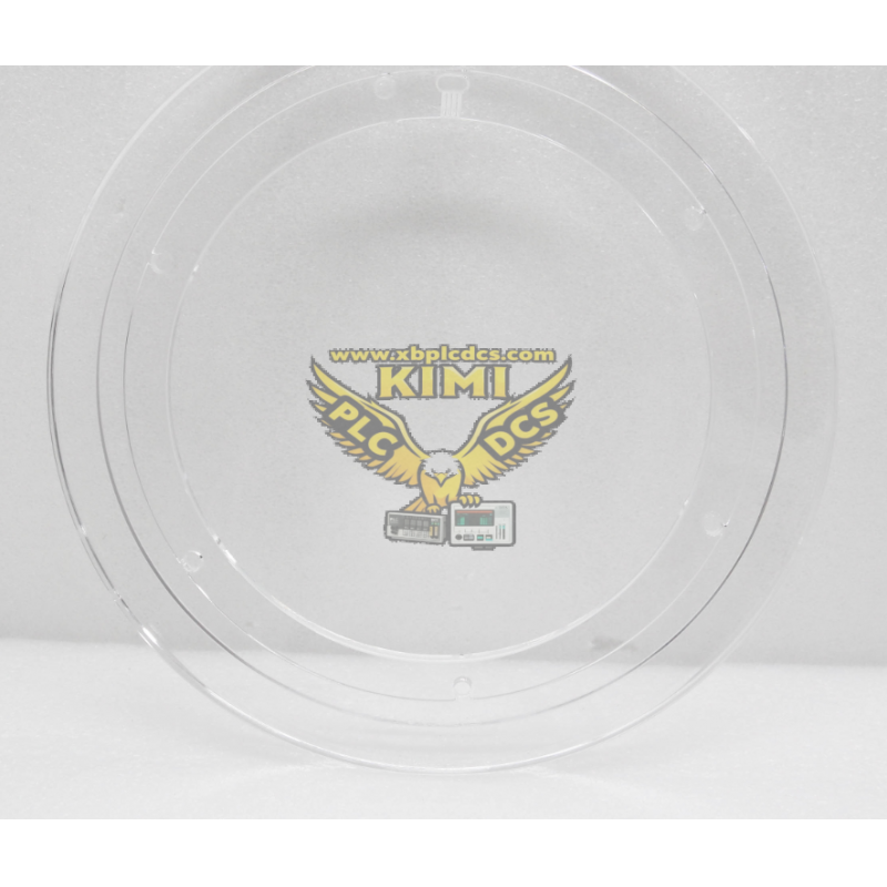
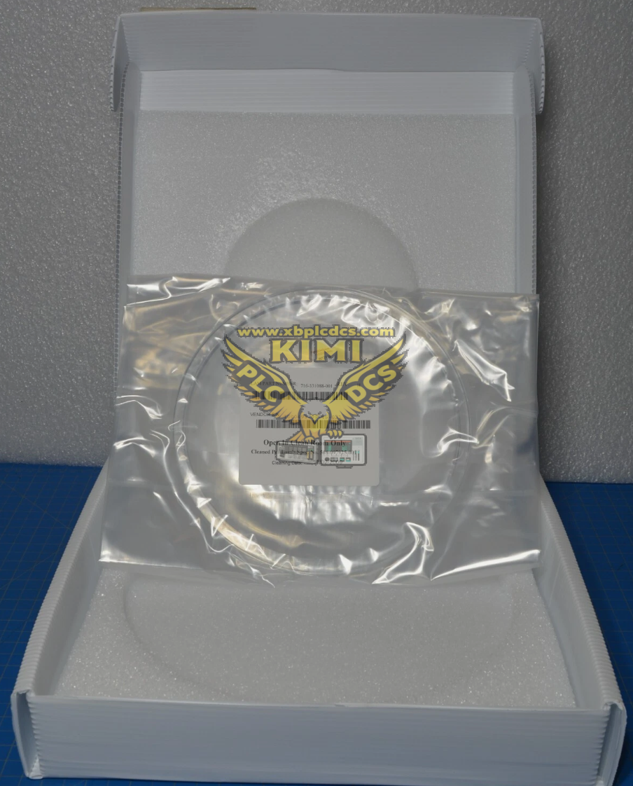
716-331088-001 is an OEM quartz Edge Ring exclusively produced by Lam Research for 200mm (8-inch) NCH ICP plasma etch chambers, full formal description: EDGE RING, 8", ES, NCH, TOP, QTZ. It is installed on the upper side of the electrostatic chuck surrounding the 8-inch wafer edge, acting as a critical quartz dielectric component to shape plasma at wafer perimeter.
- Manufactured from high-purity fused quartz (QTZ), outstanding resistance to fluorine/chlorine reactive plasma corrosion, low sputtering rate compared to ceramic materials.
- Precision annular geometry customized for NCH series etch platforms, dedicated top-position edge ring matched with bottom confinement ring assembly (716-443084-003) and top confinement ring (716-443083-004).
- Ultra-tight cleanroom dimensional tolerances, precisely control plasma gap between wafer edge and chamber wall to balance radial plasma density distribution.
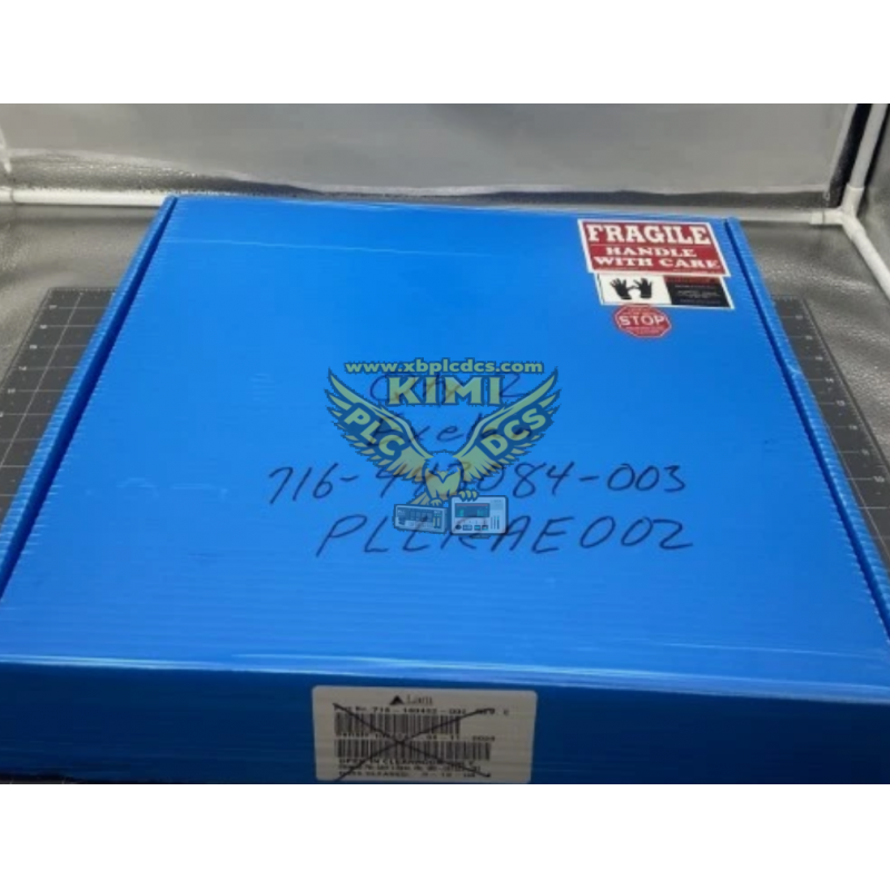
- Supplied factory-cleaned per Lam Spec 508-097925-001 aqueous cleaning standard, sealed vacuum packaging only openable inside Class 1 cleanroom to avoid particle contamination.
- Low thermal expansion quartz substrate, maintains stable edge gap dimension under repeated thermal cycling during continuous wafer batch production.
Lightweight design (0.55kg) with locating alignment notches for repeatable, zero-offset mounting on ESC edge seat.
2. Core Product Functions
- Wafer Edge Plasma Profile Tuning: Quartz dielectric material homogenizes RF electric field at wafer edge, eliminates edge rounding, trench depth offset and center-edge etch non-uniformity defects for 8-inch silicon wafers.
- Plasma Confinement Auxiliary Barrier: Cooperates with upper/lower confinement rings to block lateral plasma leakage toward chamber liner, suppress parasitic sidewall etching and reduce process micro-loading effect.
- Particle Reduction Barrier: High-purity quartz minimizes material sputtering under high-energy plasma, drastically lowers wafer particle defect count versus aluminum or coated ceramic alternatives.
- Uniform Exhaust Gas Flow Regulation: Engineered peripheral gap structure balances vacuum pumping velocity around wafer edge, stabilizes chamber pressure and eliminates radial pressure gradient drift during etching recipes.
- RF Plasma Stability Improvement: High-insulation quartz suppresses localized plasma arcing and unstable RF matching, enables consistent plasma ignition when switching different etch/deposition process recipes.
- Process Repeatability Guarantee: Fixed gap geometry maintains consistent gas flow impedance batch-to-batch, stabilizing etch rate and film thickness uniformity without frequent MFC/RF parameter re-calibration.
3. Typical Application Scenarios
- Lam Research NCH inductively coupled plasma etch chambers for legacy 200mm (8-inch) logic, memory and power semiconductor wafer manufacturing.
- High-aspect ratio dielectric etching, polysilicon gate etching and shallow trench isolation (STI) process chambers requiring strict edge uniformity control.
- Semiconductor cleanroom mass production fabs with continuous 8-inch wafer batch processing under high RF power plasma operating environments.
- Chamber preventive maintenance (PM) spare replacement to restore edge plasma tuning performance after long-term plasma erosion and quartz surface roughening.
- Full plasma confinement assembly matching: paired with 716-443090-002 upper gas inlet ring, 716-443083-004 top confinement ring and 716-443084-003 bottom confinement ring.
4. Common Issues & Troubleshooting
Issue 1: Severe center-to-edge etch rate deviation on 8-inch wafers
Root Causes: Polymer byproduct deposition blocking peripheral flow gaps, uneven plasma sputtering roughening quartz surface, misaligned installation offsetting ring symmetry. Solutions: Perform wet chemical stripping to fully clean all gap channels, inspect surface erosion depth, re-lock alignment notches fully onto ESC mounting seat.
Issue 2: Sharp rise in wafer surface particle contamination defects
Root Causes: Cracked/chipped quartz ring during chamber maintenance, deep surface pitting from long plasma bombardment, residual polymer flaking off quartz surface. Solutions: Replace 716-331088-001 once visible cracks or heavy roughening appear, adopt soft non-abrasive PTFE handling fixtures during PM.
Issue 3: Frequent intermittent plasma arc discharge and unstable RF matching
Root Causes: Uneven edge gap clearance causing localized high plasma density, thick polymer deposits accumulating static charge on quartz dielectric surface. Solutions: Full ultrasonic cleaning of all peripheral flow passages, inspect complete ring surface integrity, swap new quartz edge ring for heavily degraded units.
Issue 4: Obvious process recipe drift after hundreds of production batches
Root Causes: Gradual widening of peripheral flow gaps caused by continuous quartz sputtering, altering exhaust flow impedance and edge plasma confinement range. Solutions: Follow fab predefined PM cycle to replace the quartz edge ring, re-calibrate gas mass flow controllers and RF matching parameters post-replacement.
Issue 5: Unstable chamber vacuum pressure during etching process runs
Root Causes: Partial blockage of peripheral pumping gaps by polymer residues, foreign particles trapped between ring bottom sealing surface and ESC edge. Solutions: Deep clean all internal flow channels, fully wipe ESC contact surfaces before reinstallation, inspect matched edge O-ring seal integrity simultaneously.