

News
Featured

Contact Us
Contact: POWER DUKE
Phone: +86 18059884790
E-mail: plc66@qq.com
Add: fujian xiamen
- Warehouse: Spot
- Warranty: 365 days
- Quality: Original module
- Condition: New
- Shipping method: Courier delivery
- Contact person: LI MING
- Contact number: +86 18059884790
- WeChat:18059884790
- E-mail: plc66@qq.com
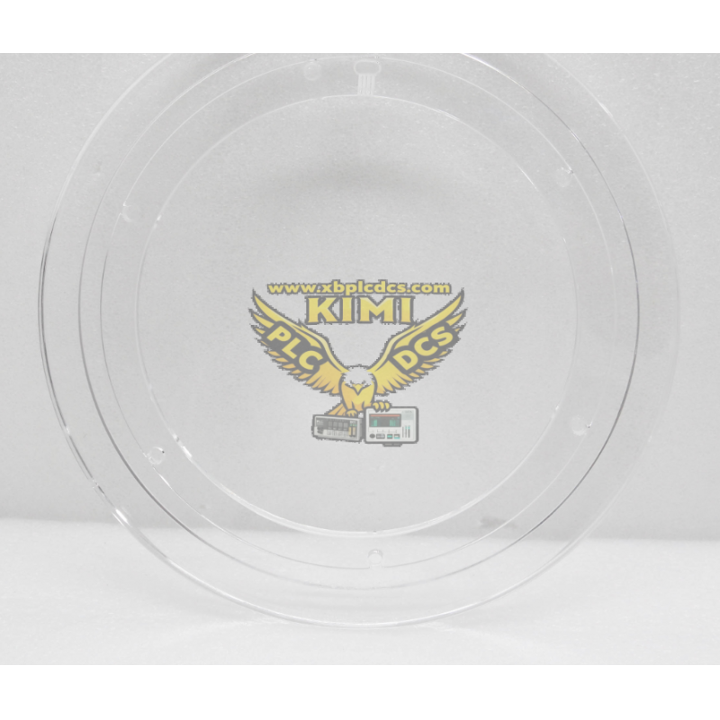
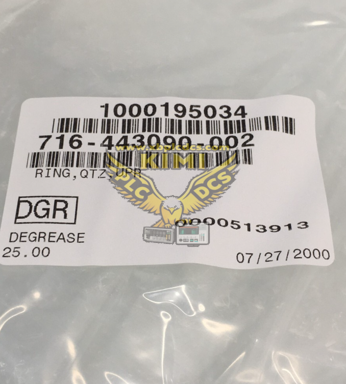
LAM 716-443090-002 Upper Gas Inlet Ring
1. Product Description
716-443090-002 is an original OEM chamber component manufactured exclusively for Lam Research semiconductor etch and thin-film deposition processing tools, named Upper Gas Inlet Ring. It is a core gas distribution hardware installed inside the process vacuum chamber, responsible for uniform delivery of process, purge and carrier gases across the wafer surface during plasma etching and deposition cycles.
- Precision machined metal alloy ring with micro-sized gas injection orifice arrays distributed in concentric circular patterns to achieve homogeneous gas flow distribution on 200mm / 300mm silicon wafers.
- Surface treated with anti-corrosion and plasma-resistant coating to resist erosion from fluorine, chlorine and other reactive etching chemistries under high-energy plasma environments.
- Integrated sealing grooves and locating alignment notches for precise mechanical positioning and vacuum tight sealing when assembled to upper chamber gas manifold assemblies.
- Conforms to strict semiconductor cleanroom cleanliness standards, precision dimensional tolerances to eliminate gas flow skew that causes uneven wafer etching rate.
- Customized LAM part revision optimized for high-power RF plasma chambers, compatible with LAM Rainbow, Exelan and Versys series processing platforms.
Designed for controlled thermal cycling inside vacuum chambers, maintains stable dimensional stability under repeated heating and cooling process cycles.
2. Core Product Functions
- Uniform Process Gas Dispersion: Distribute reactive etchant gases, inert purge gases and dilution carrier gases evenly across the entire wafer plane via precision micro-orifices, ensuring consistent etching depth and film thickness uniformity across wafer surface.
- Vacuum Chamber Sealing & Gas Isolation: Forms a sealed interface between upper gas supply manifold and plasma reaction cavity, preventing gas leakage and cross-contamination of different process chemistries inside vacuum chamber.
- Plasma Stability Control: Regulates gas injection velocity and spatial distribution to stabilize plasma density distribution, eliminating process defects such as micro-loading, etch skew and edge-to-center wafer profile deviation.
- Thermal Buffer for Chamber Environment: Acts as a heat transfer buffer between heated gas delivery lines and cool chamber walls, avoiding premature gas condensation and particle generation inside process cavity.
- Process Repeatability Assurance: Fixed orifice layout and flow impedance design guarantee identical gas flow profiles batch-to-batch, maintaining consistent semiconductor process recipe performance for mass wafer production.
- Particle Reduction: Smooth plasma-resistant coating minimizes sputtering and material shedding during long plasma exposure, reducing wafer defect counts induced by chamber particle contamination.
3. Typical Application Scenarios
- Lam Research inductively coupled plasma (ICP) etch chambers for logic, memory and power semiconductor wafer manufacturing.
- High aspect ratio dielectric and conductor etching processes for advanced node semiconductor devices.
- Wafer thin-film deposition pre-treatment and surface passivation process chambers requiring precise gas distribution control.
- 200mm / 300mm cleanroom production fabs with continuous batch wafer processing under high RF plasma power operating conditions.
- Semiconductor fab chamber preventive maintenance (PM) spare parts replacement to restore chamber gas flow uniformity after long-term plasma erosion.
4. Common Issues & Troubleshooting
Issue 1: Uneven wafer etch rate, center-edge profile deviation
Root Causes: Partial clogging of micro gas orifices by polymer byproduct deposition, uneven plasma erosion of ring surface coating, misaligned installation offsetting gas injection pattern. Solutions: Perform wet chemical clean to remove polymer residues from all orifices, inspect surface coating wear, re-align locating notches and fully seat ring to manifold seal surface.
Issue 2: Increased particle contamination and wafer defect counts
Root Causes: Damaged anti-plasma coating with spalling, surface pitting from long reactive plasma exposure, scratched ring surface during PM handling. Solutions: Replace the 716-443090-002 gas inlet ring once coating degradation is detected, implement anti-scratch handling protocols during chamber maintenance.
Issue 3: Vacuum pressure instability and gas leakage alarm during process run
Root Causes: Worn sealing groove on ring edge, damaged interface O-ring mating surface, foreign particles trapped between ring and manifold sealing face. Solutions: Polish ring sealing surface, replace matched chamber O-rings, fully purge and clean contact surfaces before reinstallation.
Issue 4: Process recipe drift after multiple production batches
Root Causes: Gradual enlargement of gas orifices due to plasma sputtering altering gas flow impedance. Solutions: Schedule periodic replacement of upper gas inlet ring according to fab PM cycle, re-calibrate gas mass flow controllers after ring swap.
Issue 5: Plasma ignition instability and intermittent arc discharge inside chamber
Root Causes: Uneven gas injection distribution from blocked orifices causing localized high gas concentration, exposed conductive substrate from coating loss. Solutions: Full orifice unclog cleaning, inspect coating integrity, replace ring if severe substrate exposure is present.