

Product
Product
News
Featured
Contact Us
Contact: POWER DUKE
Phone: +86 18059884790
E-mail: plc66@qq.com
Add: fujian xiamen
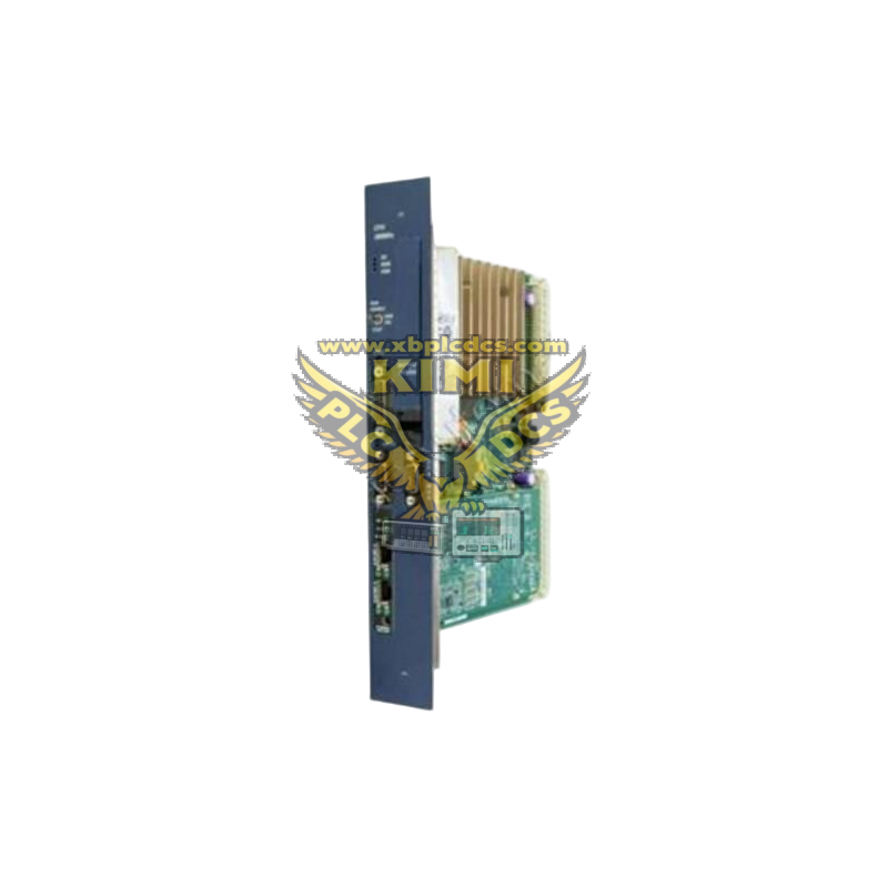
Applied Materials 0021-16781--kimi
- Warehouse: Spot
- Warranty: 365 days
- Quality: Original module
- Condition: New
- Shipping method: Courier delivery
- Contact person: LI MING
- Contact number: +86 18059884790
- WeChat:18059884790
- E-mail: plc66@qq.com
Product Description
Applied Materials 0021-16781
Product Description
0021-16781 is an upper shield component (Shield Upper, Rev 2.0 Sip Cu, 300mm) manufactured by Applied Materials for semiconductor wafer processing chambers. It is a copper-based shielding part designed for 300mm wafer platforms, used inside deposition process chambers to define plasma boundaries and protect chamber hardware from unwanted material deposition.

Product Functions
- Forms physical and plasma shielding inside the process chamber during copper deposition.
- Controls plasma distribution to ensure uniform thin-film deposition on 300mm silicon wafers.
- Reduces sputter deposition on inner chamber walls and protects other chamber components.
- Maintains stable chamber geometry to preserve process repeatability and wafer yield.
Application Scenarios
- Applied Materials Endura / Centura 300mm semiconductor processing platforms.
- Copper SIP deposition chambers for advanced wafer metallization processes.
- Semiconductor fabs for logic and memory chip manufacturing.
Frequently Asked Issues
- Surface particle contamination: Copper shield surface accumulates deposits, causing wafer defects; requires periodic cleaning or replacement.
- Physical erosion: Long-term plasma bombardment leads to shield wear, degrading plasma uniformity.
- Deformation: Thermal cycling may cause warping, altering chamber spacing and process drift.
- Improper installation: Misalignment causes arcing, chamber leaks or inconsistent deposition results.
Related recommendations