

Product
Product
News
Featured
Contact Us
Contact: POWER DUKE
Phone: +86 18059884790
E-mail: plc66@qq.com
Add: fujian xiamen
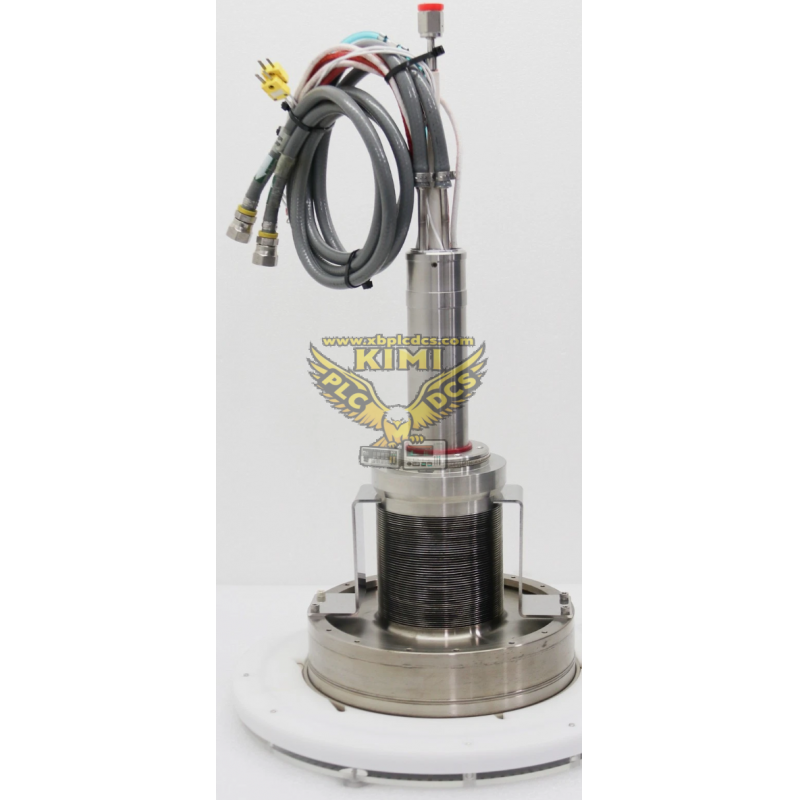
Applied Materials 0190‑45353 High‑Voltage Bias PCB Assembly
- Warehouse: Spot
- Warranty: 365 days
- Quality: Original module
- Condition: New
- Shipping method: Courier delivery
- Contact person: LI MING
- Contact number: +86 18059884790
- WeChat:18059884790
- E-mail: plc66@qq.com
Product Description
Applied Materials 0190‑45353 High‑Voltage Bias PCB Assembly
Product Description
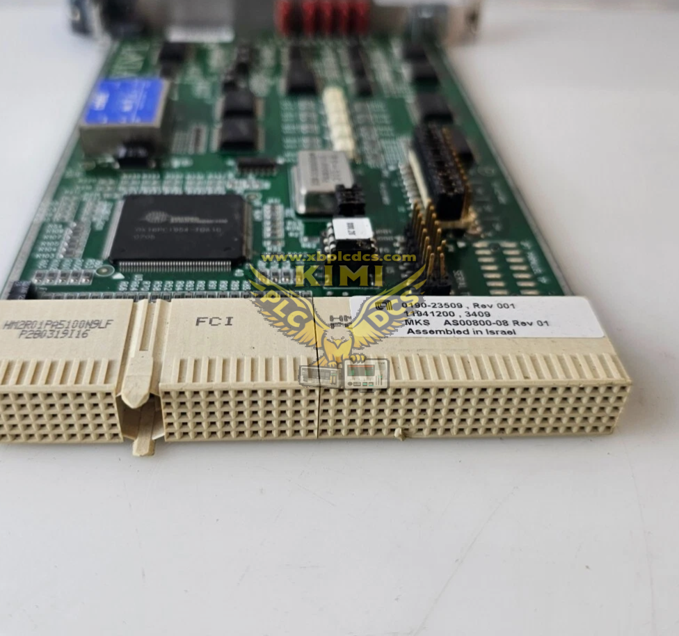
0190‑45353 is a high‑voltage bias control PCA board assembly for Applied Materials Endura / Centura semiconductor cluster tools. This PCB provides programmable high‑voltage bias output, analog sensing, arc‑quenching detection and isolation signal conditioning for plasma process chambers. It converts low‑level tool host set‑points into controlled high‑voltage bias signals for electrostatic chuck (ESC) or plasma biasing elements. Integrated over‑voltage, over‑current and arc‑fault detection circuits protect chamber hardware and wafer substrates during PVD, Etch and CVD production recipes.
Key Functions
- High‑voltage bias output regulation for electrostatic chuck and plasma bias electrode, configurable voltage range
- Real‑time arc strike detection and fast hardware arc quenching to suppress plasma arc damage to wafers and chamber parts
- Voltage and current closed‑loop sensing, analog telemetry feedback back to tool main controller
- Hardware interlock circuits: over‑voltage, over‑current, over‑temperature fault latch‑off protection
- Isolated digital / analog interface to receive recipe set‑points; report fault flags, measured voltage‑current values to system host
- Built‑in diagnostic monitoring counters for arc‑event logging, supporting process troubleshooting and predictive maintenance
Application Scenarios
- Applied Materials Endura and Centura cluster processing platforms
- PVD physical vapor deposition chamber ESC bias control subsystem
- Plasma etch and CVD thin‑film deposition process modules
- 200 mm wafer high‑volume clean‑room manufacturing environment
Common Issues & FAQ
- Frequent arc‑detect trips during plasma ignition: Inspect high‑voltage cable insulation and feed‑through condition; verify chamber interior for contamination or micro‑arcing sources; check board arc‑detection threshold parameters via service menu; inspect on‑board high‑voltage components for degradation.
- Bias voltage cannot reach recipe set‑point: Check input power supply rail; inspect sense‑loop wiring continuity; perform offset and gain calibration; check for partial component derating under thermal load.
- Over‑current fault alarm: Check for chamber load short‑circuit; verify ESC chuck insulation resistance; inspect PCB for trace or capacitor damage.
- No telemetry / host communication failure: Inspect signal harness and connector pin integrity; confirm board enable interlock status; check fuse status on auxiliary power input.
- Refurbished unit note: After replacement, perform high‑voltage withstand test, full‑range bias calibration, arc‑fault interlock validation and plasma recipe test before releasing to wafer production.
Related recommendations