

News
Featured
Contact Us
Contact: POWER DUKE
Phone: +86 18059884790
E-mail: plc66@qq.com
Add: fujian xiamen
- Warehouse: Spot
- Warranty: 365 days
- Quality: Original module
- Condition: New
- Shipping method: Courier delivery
- Contact person: LI MING
- Contact number: +86 18059884790
- WeChat:18059884790
- E-mail: plc66@qq.com
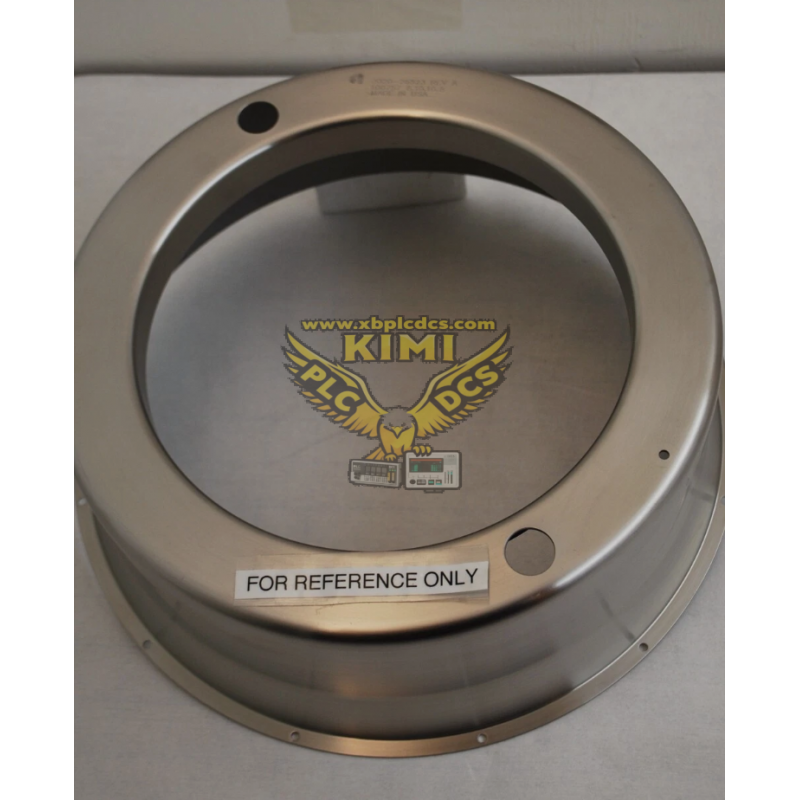
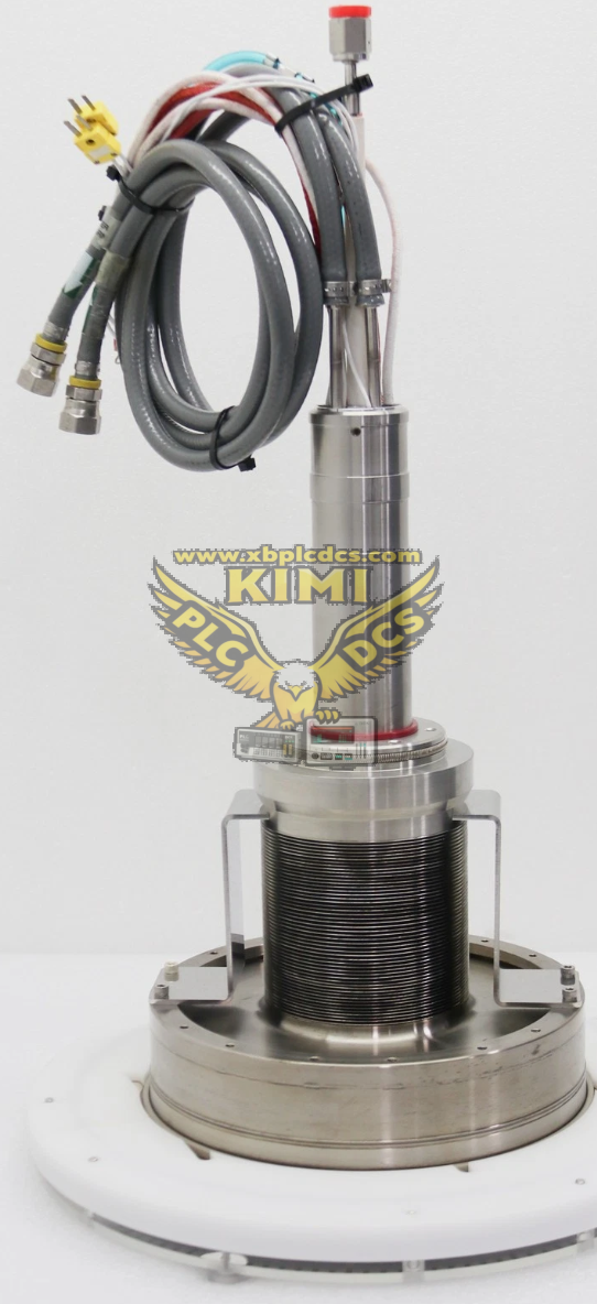
Applied Materials 0010-27431 Pedestal Assembly, 300mm PIB HT BESC
Product Description
The 0010-27431 is a 300mm high-temperature pedestal (ESC / wafer base) assembly manufactured by Applied Materials for semiconductor vacuum process chambers. This integrated assembly includes electrostatic chuck body, embedded multi-zone heater, RTD temperature sensors, gas backside cooling channels, feedthrough wiring and bellows lifting structure. It is designed to hold, electrostatically clamp and heat 300mm silicon wafers under high vacuum and plasma environment. It uses ultra-clean vacuum-grade materials with low particle emission and low outgassing, compatible with AMAT Endura / Producer PVD or CVD process platforms. Available inventory includes surplus and refurbished units for fab chamber maintenance and rebuild.
Product Functions
- Mechanically support and electrostatically clamp 300mm silicon wafer inside high-vacuum process chamber during thin-film deposition or etch recipes
- Multi-zone embedded heater provides precise and uniform substrate temperature control across wafer surface for stable semiconductor process performance
- Backside helium gas delivery channel for conductive cooling between wafer and chuck to enhance thermal transfer and temperature uniformity
- Built-in RTD temperature sensors feed real-time temperature readings to chamber thermal controller for closed-loop thermal regulation
- Integrated bellows lifting mechanism for wafer pick-and-place movement, to lift/lower wafer during wafer transfer sequence
- Electrostatic clamping control to secure wafer firmly, prevent wafer shifting under plasma and thermal stress
- Provide hardware fault signals to tool host for interlock protection on over-temperature, heater open circuit and ESC leakage faults
Application Scenarios
- 300mm wafer PVD / CVD vacuum process chambers on Applied Materials Endura and Producer platforms
- Metal barrier layer, copper and dielectric thin film deposition processes for advanced semiconductor manufacturing
- Spare replacement for damaged or degraded 0010-27431 pedestal assemblies in production wafer fabrication tools
- Chamber preventive maintenance, wet clean, overhaul and chamber rebuild projects in 12-inch semiconductor fabs
- Process recipe qualification and wafer temperature tuning for thin-film uniformity optimization
- Spare parts inventory for semiconductor equipment service vendors and wafer manufacturing factories
Common Problems
- Heater open circuit: burnout of embedded heating elements caused by repeated thermal cycling and plasma radiation erosion
- ESC clamping failure: dielectric layer degradation, leakage current increase, cannot hold wafer stably
- Temperature measurement drift: built-in RTD sensor aging or damage of internal feedthrough wiring
- Backside helium gas leakage: seal aging, gas channel blockage by process by-product deposits
- Particle contamination: chuck surface coating peeling, ceramic cracking, leading to wafer yield loss
- Bellows lifting malfunction: mechanical fatigue of bellows, stuck movement or vacuum leakage at bellow joint
- Refurbished unit risk: residual dielectric wear; full leakage test, temperature mapping and ESC leakage test required before installation into production chamber