

News
Featured


Contact Us
Contact: POWER DUKE
Phone: +86 18059884790
E-mail: plc66@qq.com
Add: fujian xiamen
- Warehouse: Spot
- Warranty: 365 days
- Quality: Original module
- Condition: New
- Shipping method: Courier delivery
- Contact person: LI MING
- Contact number: +86 18059884790
- WeChat:18059884790
- E-mail: plc66@qq.com
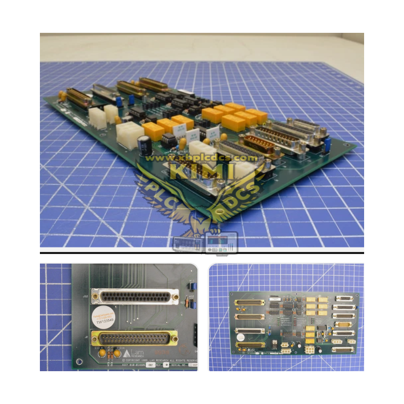
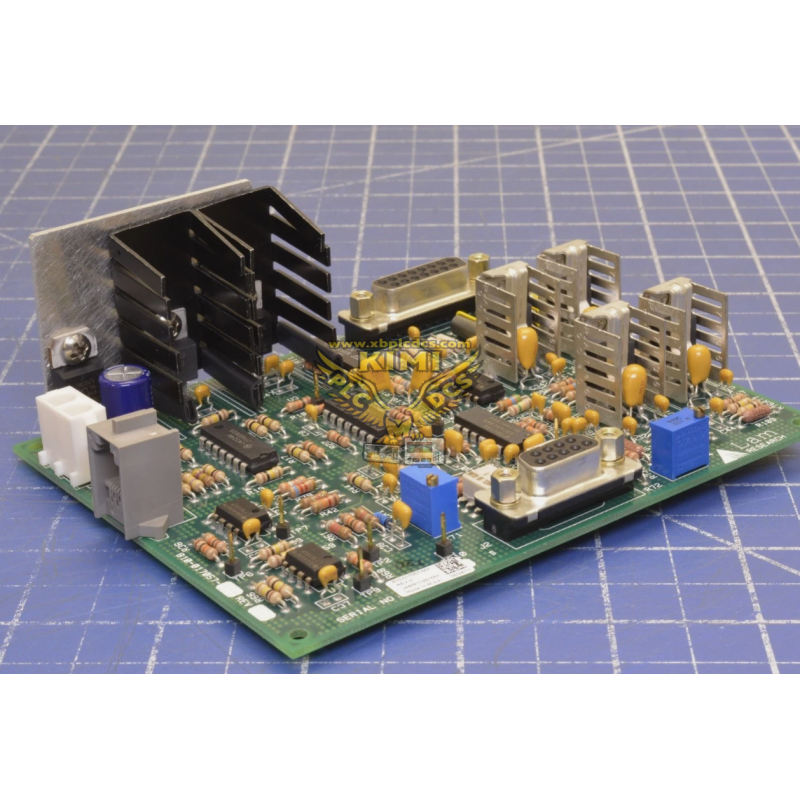
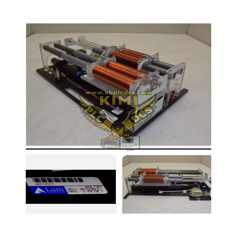
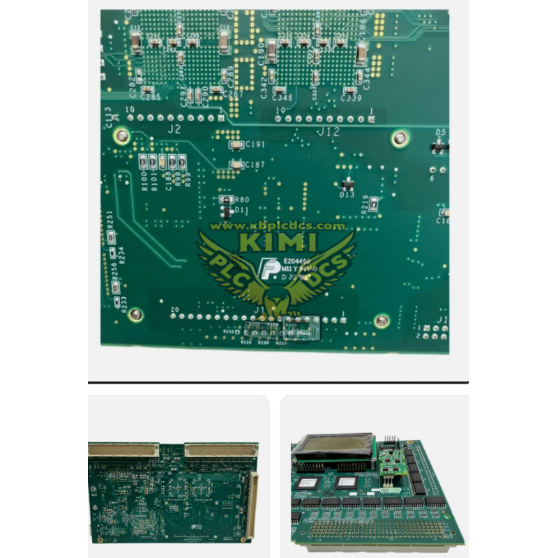
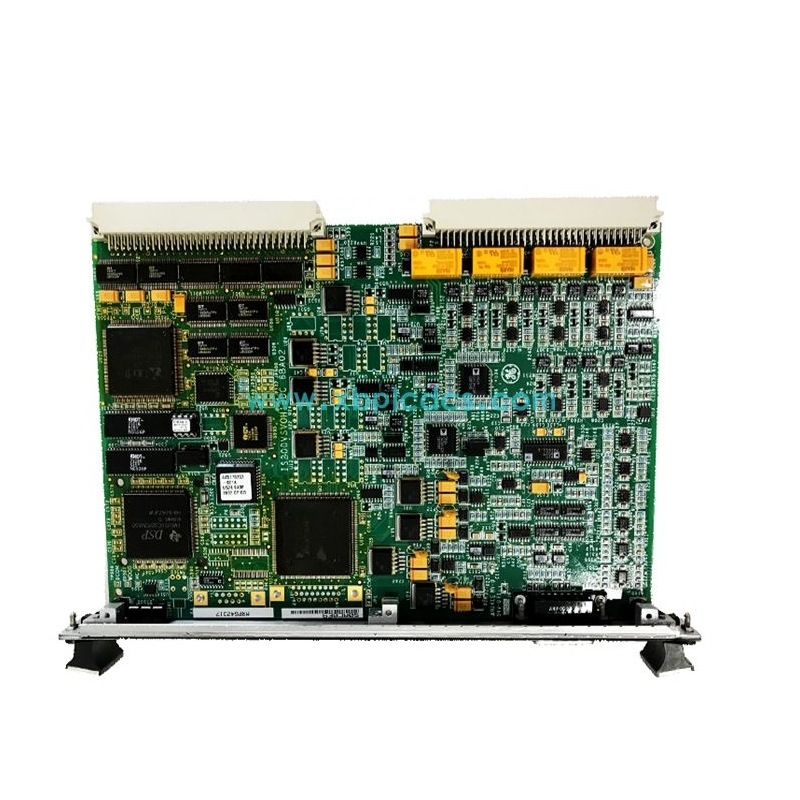
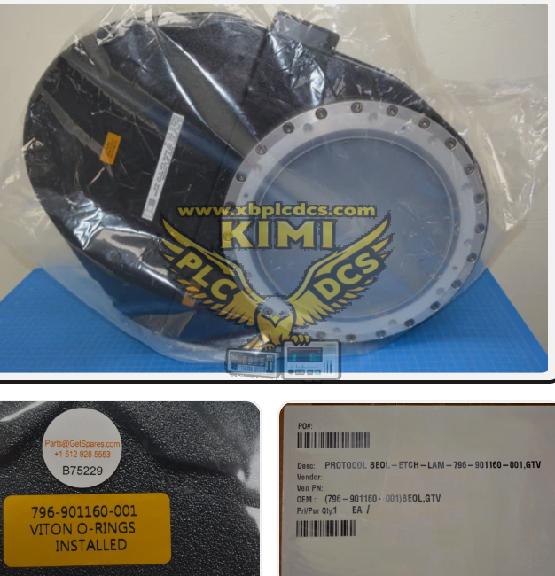
Lam Research 796-901160-001 Semiconductor Equipment PCB Assembly
Product Description
796-901160-001 is a printed circuit board assembly manufactured by Lam Research for semiconductor wafer processing etch tools. This board is a subsystem interface control card used inside Lam plasma etching equipment. It handles analog signal acquisition, sensor feedback collection and drive command output for gas modules, vacuum or pressure control subsystems. The PCB assembly comes with soldered components, undergoes factory burn-in testing and ESD protection treatment. Designed for 19-inch rack installation inside the semiconductor process chamber controller cabinet, it serves as a spare replacement part for fab production tools.
Key Functions
- Analog and digital signal acquisition from process sensors and actuators
- Signal conditioning and feedback control for gas flow, pressure or vacuum subsystems
- Data communication with main VME host controller of the etch system
- On-board circuit fault detection and status feedback for tool host software
- ESD protected, anti-vibration design to meet fab cleanroom operating conditions
- Standard rack slot mounting for Lam plasma etcher equipment chassis
- Full component pre-assembled, ready for direct replacement as spare part
Application Scenarios
- Lam Research plasma etch wafer processing semiconductor tools
- Cleanroom fab equipment maintenance, spare parts swap and repair
- Process chamber auxiliary monitoring and control subsystem
- Semiconductor production line equipment upgrade and refurbishment project
FAQ
Q: Who manufactures 796-901160-001?
A: Lam Research, USA semiconductor equipment OEM.
Q: What equipment is this PCB used on?
A: Lam plasma etch wafer processing tools in semiconductor fabs.
Q: What is the main role of this assembly?
A: Collect sensor signals and communicate with the main system for process chamber auxiliary control.