

News
Featured


Contact Us
Contact: POWER DUKE
Phone: +86 18059884790
E-mail: plc66@qq.com
Add: fujian xiamen
- Warehouse: Spot
- Warranty: 365 days
- Quality: Original module
- Condition: New
- Shipping method: Courier delivery
- Contact person: LI MING
- Contact number: +86 18059884790
- WeChat:18059884790
- E-mail: plc66@qq.com
Lam Research 710-809156-000 Semiconductor Equipment PCB Assembly
Product Description
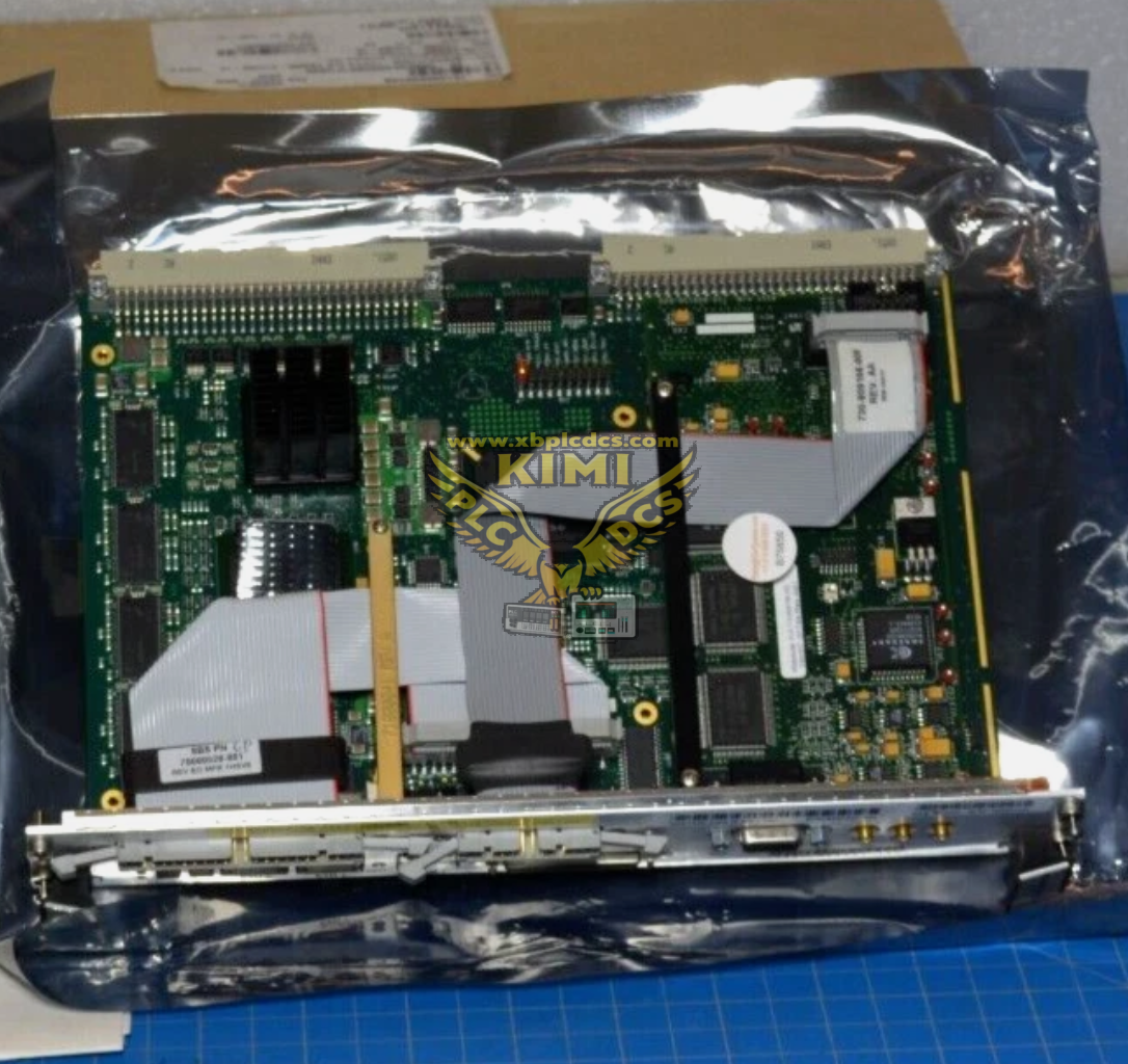
710-809156-000 is a printed circuit board assembly from Lam Research, used in Lam plasma etch wafer processing semiconductor tools. This board serves as a precision analog/digital interface card, responsible for chamber sensor signal acquisition, actuator driving and inter-board communication inside the process tool controller. It is fully assembled with electronic components, manufactured with strict ESD control and factory burn-in test. Designed for installation inside the equipment control cabinet, it is widely used as OEM spare replacement part for semiconductor fab production tools.
Key Functions
- High-precision analog signal collection from chamber pressure, temperature and gas sensors
- Digital I/O control for pneumatic valves, vacuum interlock and chamber auxiliary actuators
- High-speed data communication with the main system controller for process command exchange
- On-board self-diagnosis circuit for hardware fault detection and status reporting
- ESD protection and anti-vibration design, suitable for cleanroom fab operating environment
- Standard rack slot mounting inside Lam etcher equipment chassis
- Pre-assembled PCB assembly for direct replacement during equipment maintenance
Application Scenarios
- Lam Research plasma etching wafer processing semiconductor equipment
- Semiconductor cleanroom fab equipment maintenance and spare parts swapping
- Process chamber monitoring, gas and vacuum control subsystem
- Fab tool refurbishment, upgrade and spare inventory backup
FAQ
Q: Who manufactures 710-809156-000?
A: Lam Research, USA semiconductor equipment OEM.
Q: What equipment is this PCB applied to?
A: Lam plasma etch wafer processing tools in semiconductor fabrication plants.
Q: What is the main purpose of this board?
A: Collect chamber sensor signals, control field actuators and communicate with the main tool controller.